Shin-Etsu Chemical, a leading company in semiconductor technology, has announced a groundbreaking development in the manufacturing process of semiconductor package substrates. The company has introduced new equipment utilizing a unique manufacturing method that aims to revolutionize the back end process of semiconductor production.
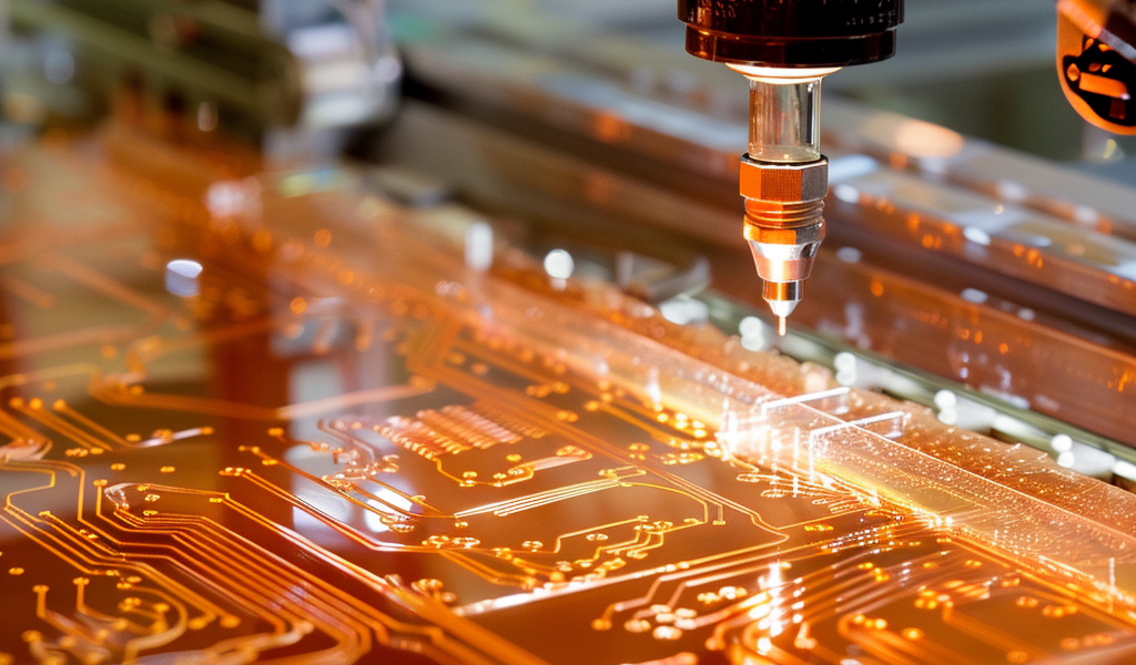
The newly developed equipment by Shin-Etsu Chemical incorporates an innovative approach using excimer laser technology, known as the Shin-Etsu dual damascene method. This method, similar to the process utilized in the front end of semiconductor manufacturing, eliminates the need for an interposer in the package substrate manufacturing process. By directly integrating the functions of an interposer into the package substrate, this advancement allows for enhanced microfabrication capabilities that were previously unattainable.
One of the key advantages of this new manufacturing method is the significant reduction in costs and capital investment. By bypassing the traditional photoresist process in package substrate manufacturing, Shin-Etsu Chemical’s technology not only streamlines the production process but also paves the way for further cost savings in chiplet development.
The implementation of the Shin-Etsu dual damascene method holds great promise for the semiconductor industry, particularly in the realm of chiplet technology. Chiplets, which involve the assembly of singulated circuits in a package, have emerged as a cost-effective solution for high-performance semiconductors. With the elimination of the interposer through Shin-Etsu’s method, the assembly process for chiplets is simplified, leading to reduced manufacturing costs and enhanced efficiency.
Through the utilization of advanced microfabrication techniques, the equipment developed by Shin-Etsu Chemical enables the direct formation of intricate electric circuit patterns within the organic insulation layers of a multi-layered package substrate. This process, combined with copper plating for circuit formation, leverages excimer laser technology to achieve precise and efficient large-area circuit patterning.
Overall, the Shin-Etsu dual damascene method represents a significant leap forward in semiconductor manufacturing, offering a more streamlined and cost-effective approach to producing advanced semiconductors with chiplet technology. By eliminating the need for an interposer and enhancing microfabrication capabilities, Shin-Etsu Chemical’s innovative equipment is poised to drive efficiency and cost savings in the semiconductor industry.